


DI(WH)Y Lab Power Supply
Back to projectsOne of the projects that I started in December of '21 of junior year was a lab power supply. I was mainly curious about how lab power supplies can regulate constant current or constant voltage, and I was a little bored, so I started designing a schematic for the DC to DC output stage of a lab power supply. I wanted up to 60V and 10A output, and chose the LM5118 controller IC, because of an application note that described a CC/CV regulator using the LM5117, but couldn't find any in stock.
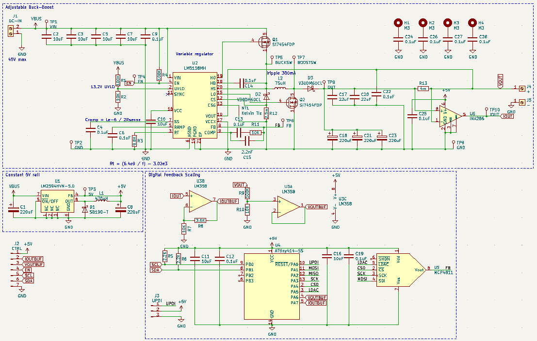 The final schematic
The Theory
Voltage regulators keep the output voltage constant regardless of changes in load by comparing a constant voltage reference to a voltage feedback signal, which is the output of a voltage divider from the output of the buck converter. The voltage divider scales the feedback voltage to a known proportion to the output voltage, so if we keep feedback equal to a reference voltage, we are effectively keeping the output voltage equal to a certain setpoint, a multiple of the reference voltage. Changing the resistances of the voltage divider changes the scaling factor, changing the output voltage setpoint without having to change the reference voltage. To be able to adjust output, we use a potentiometer as the feedback voltage divider.
The comparison is done by the compensator stage, which outputs an analog voltage into a comparator stage that compares the voltage to a sawtooth wave (called Vramp in the figure below) resulting in the output being a square wave with the PWM duty cycle proportional to the compensator stage's output. The square wave feeds into the gate of the MOSFET that switches current into the inductor. When output voltage is higher than the setpoint (Vfb > Vref), the PWM duty cycle decreases, which reduces the switch duty cycle and results in a lower voltage. When output is lower than the setpoint, the opposite occurs.
 Image credit: Microchip
Almost all voltage regulators also have a current regulation feature, but this is really just an over current protection so that the voltage feedback doesn't fry the switch in the case of a dead short or overdraw. This current regulation feature measures the inductor current, and if it goes over a certain threshold, turns off the switch until the current goes below the threshold. This has the effect of a constant current regulator rather than a latching overcurrent protection, as the output voltage will decrease until the current is just under the overcurrent threshold, not necessarily going to zero.
To implement an adjustable constant current and constant voltage regulator, I chose to analog OR a current sense output with the voltage output. I added a current shunt and current sense amplifier, then scaled the output (in the same way that Vfb is scaled from output voltage), then analog OR'ed this output with the Vfb from the voltage feedback. By analog ORing, the greater of the two feedback voltages is compared to the reference voltage, so the switch duty cycle will decrease if the output voltage is greater than the output voltage setpoint, or if the output current is greater than the output current setpoint. This has the effect we want, because really we are only limited by one at a time; voltage OR current.
Alternative (and probably better) Methods
There are other ways to implement CC/CV, but the main idea is the same. One alternative is to scale the output current and feed it back to the current sense pin used for overcurrent protection, such that OCP triggers whenever current rises above the current setpoint. This requires more components and more thought into small analog signal scaling, since it deals with voltages that must be accurate in the millivolt range.
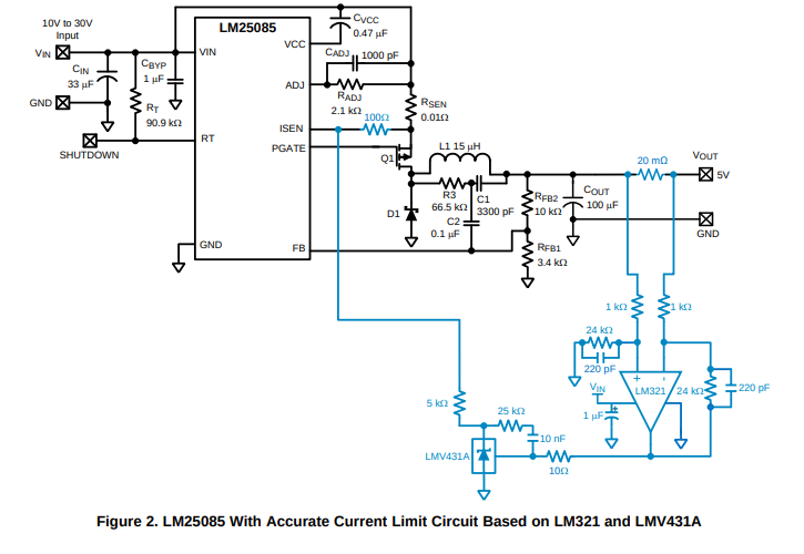 Image credit: Texas Instruments
The LM5117 application note I mentioned above eliminates one sense resistor on the output by taking advantage of the CM output pin on the 5117 to feedback the output of the 5117's internal current sense amplifier (used for OCP by measuring the current through the a shunt resistor on the low side of the switch) into the feedback pin, with a diode from the voltage feedback. Vfb is also clamped with a 431 voltage reference.
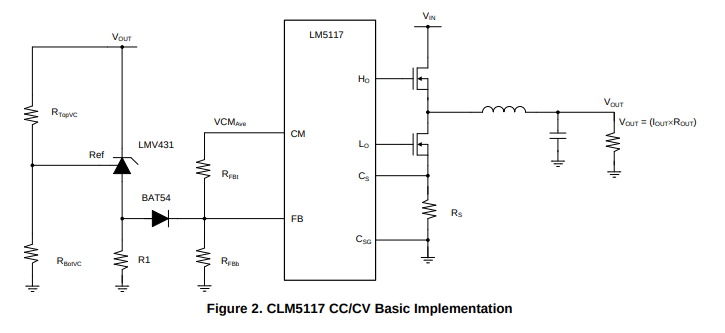 Image credit: Texas Instruments
My Implementation
I soon realized the issue with analog ORing the circuits together: there is no way to display the voltage or current setpoint. Most cheap lab power supplies don't worry about this, and just measure the output current and voltage and display those, but I wanted to be able to see what my setpoints were, especially what my current limit was. I thought about using dual gang potentiometers so that a microcontroller could measure the position of the potentiometer separately from the feedback circuitry, but that limited my potentiometer options. So I decided to try a digital feedback system, with a microcontroller reading the analog feedback voltage with an ADC, scaling in code, and outputting an analog voltage to the feedback pin of the buck converter using a DAC. In hindsight, I probably should have just used single gang potentiometers and physically marked the positions per current and voltage setting, but I learned a lot more this way.
Doing it digitally requires a lot of considerations for speed, from the analog to digital conversion to the digital processing to the analog output. Buck converter feedback traditionally uses analog circuitry to maximize the crossover frequency, or the frequency beyond which the system does not respond to changes; the frequency of noise that will not be filtered. We want to maximize crossover frequency and error amplifier gain to minimize output oscillations. The in circuit considerations were using op-amp buffers to make sure the ADC can read fast changes to either feedback voltage. I considered using an external ADC for potentially faster readings but decided against it, because the time needed for SPI transfer would have negated the conversion advantage, and the ATTiny1624 I was using already had one of the best AVR internal ADCs.
This is where I learned the most about low level microcontroller code, because port manipulation is needed to speed things up as much as possible. For example, arduino digitalWrite actually takes 50 clock cycles because of the look-up tables for the pins, while using port manipulation to set the output takes only two clock cycles. Something similar can be done for analogRead, but the time savings are not as extreme because the ADC still needs time to take the sample itself. ADC freerun is an option that continuously reads the analog input and triggers an interrupt once the digital conversion is complete, but it only works for one ADC pin at a time, making it not useful for this application. I did shorten the ADC sample time, because not much time should be needed to charge the capacitor internally thanks to the op-amp buffers. I used port manipulation and nops to control the CS pin on the DAC output in order to speed up the SPI data transfer as much as possible. Finally, there was the problem of setting the voltage and current scaling in the microcontroller. I decided to use i2c for this, accepting that during an i2c transfer, the microcontroller would be momentarily unable to perform the feedback functionality. The scalings are stored as variables within the microcontroller, so the i2c transfer only needs to happen every time the set points change.
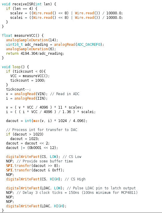 The relevant part of the microcontroller code, using an ATTiny1624
Assembly, Testing
It wouldn't be a project without putting it into practice. I routed out the PCB for the DC-DC converter, ordered the board, and ordered the components. I also didn't realize that the size of an inductor was a tradeoff, not something to maximize, so I chose a 75uH 10A inductor, which remains the largest shielded inductor I have ever got my hands on. I didn't realize that this would have made the transient response horrible unless I added more capacitors to the output, which would have made the board larger and more expensive, and would have added more points of failure.
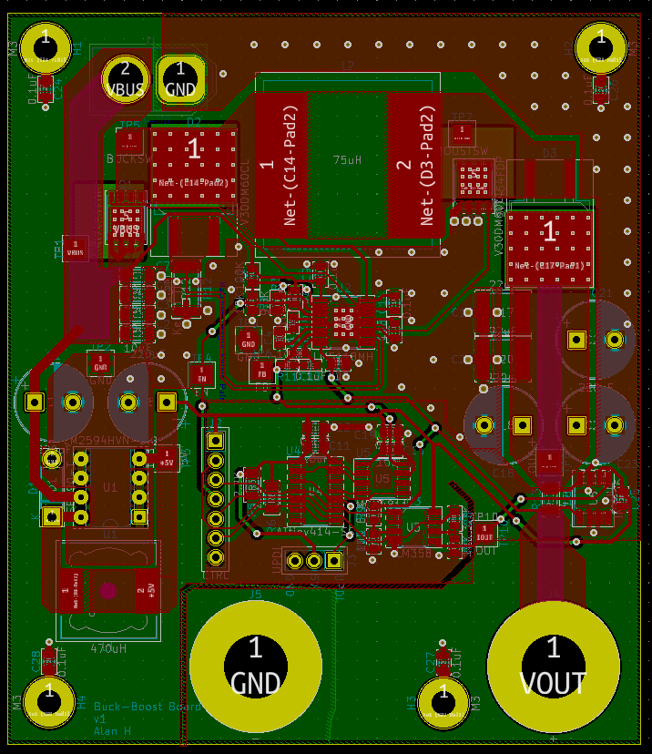 Final Layout
This was my first time doing solder reflow with a hot air station, and I spent six hours pasting the board, placing components, and soldering.
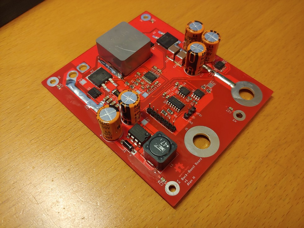 The completed assembled board
I wrote up the code and uploaded it, then brought it into school in the robo lab to test it. I plugged in power to the input, and almost immediately an output capacitor explodes. I try again (because I'm a bit of an idiot) and a second capacitor explodes. Fortunately I was in the back corner of the lab, so the smoke wasn't too visible. I checked my code, and realized my mistake: I forgot to convert the ADC 12 bit reading to a voltage when doing my scaling math. As a result, the output setpoint was over 70 volts, not the 5 I had set it to. When I brought the supply back home, replaced the broken components, and uploaded new code, I tried again, only to find out it wasn't functioning. I probed a few points, checked for dead shorts, but came up inconclusive. I tried to replace the LM5118, and it didn't help. I considered assembling a whole new board, but the jankness of my feedback solution was wearing on me, and the cost of the components led me to decide against it.
Those two exploded capacitors sat in the back of the robo lab for a few months, and my friends still tease me about it.
Conclusion
The project was not successful, and if my goal had been to design and build a working lab power supply, it would have been a failure. If that had been my goal, I should have gone for a smaller scope, for example not bothering with digital feedback and settling for analog OR, or better yet, just buying a lab power supply-they don't cost that much. But I didn't really have a solid goal with this project. I was just exploring switching voltage converters, and though I definitely wanted a 60V 10A power supply, I wasn't banking on finishing it.
In the end, I learned a lot. I learned about the operating theory of buck converters and buck-boost converters. I learned about the circuits used to regulate current and voltage. I learned about fast microcontroller code, and register manipulation on ATTiny AVRs. I got experience with pasting and reflowing SMD components with a hot air station. I had my first brush with feedback network design and the complex math, bode plots, zeros, and poles, that still puzzle me today (my second encounter was sitting in on a Power Electronics lecture at Cornell back in October). Even though the project was unfinished, and sits on my desk as a reminder to be cautious of project scope, I learned most of my power electronics theory from it. And even if it had been successful, it really wouldn't have been a good power supply. The large inductor would have made the transient response slow, compounded by the suboptimal digital feedback. I keep this project in mind whenever I think about building something rather than buying, and as an example of overscoping a project.
Last updated 26 Nov 2022